System-in-Package (SiP) Technology Analysis
As the functions of electronic products become increasingly complex, traditional integrated circuit packaging methods are gradually unable to meet the needs of miniaturization, high performance and multi-functions. As an innovative solution, System-in-Package (SiP) technology is becoming an important choice for modern electronic design because it can integrate multiple chips, passive components and other devices in a single package. This article will analyze the definition, advantages, application areas and future development direction of SiP technology.Visit DRex Electronics for more similar content on an electronic component supplier.
What is System-in-Package (SiP)?
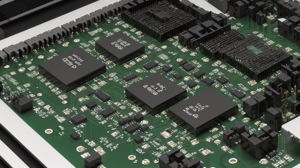
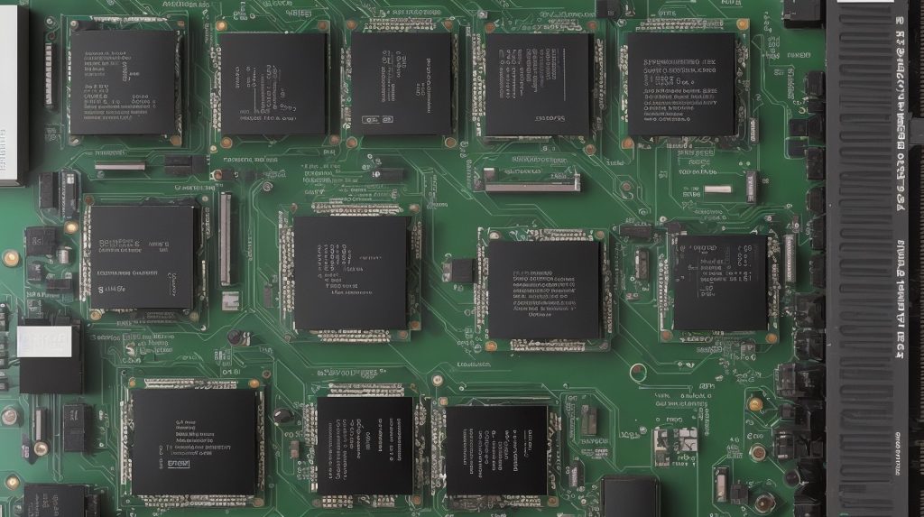
SiP is an advanced integrated packaging technology that integrates multiple chips with different functions (such as processors, memory, sensors, wireless communication modules, etc.) and their supporting passive components, such as resistors, capacitors and inductors, in one package. Compared with System-on-Chip (SoC), SiP technology does not rely on integrating all functions on a single wafer, but connects different chips together through substrates, wire bonding or flip chips through packaging processes to form a complete system function.
Advantages of System-in-Package
- High integration and miniaturization
SiP technology allows the integration of multiple chips and devices in a small package, which greatly reduces the volume and weight of the overall circuit and meets the needs of miniaturization for mobile devices, wearable devices, etc. In addition, SiP reduces the PCB area and helps to design more compact products.
- Flexible design scheme
SiP is different from SoC, which requires strict integration of all functional modules in the design stage, which has high requirements for design requirements and development cycle. SiP allows designers to integrate ready-made chips (such as components from different suppliers), which provides greater flexibility for system design and reduces development risks and costs.
- Shorter product development cycle
SiP reduces the time from design to production by encapsulating multiple existing chip components, so it can speed up the time to market. In addition, SiP technology allows independent optimization and development of each functional module, further improving development efficiency.
- Performance optimization and functional diversification
By integrating chips and components with different functions in the package, SiP technology not only improves the performance of the system, but also integrates multiple functional modules, such as wireless communication modules and sensors, to achieve the design of multi-functional devices.
Application fields of system-level packaging
SiP technology is widely used in many fields, especially in scenarios with high requirements for miniaturization, low power consumption and multi-functional integration:
- Smartphones and mobile devices
In smartphones, SiP can integrate processors, memory, communication modules and sensors, etc., so that the device has powerful computing power and functional integration while maintaining miniaturization.
- Wearable devices
Wearable devices such as smart watches and health monitoring devices have extremely high requirements for miniaturization and low power consumption. SiP technology can effectively integrate multiple sensors and wireless communication modules to meet the needs of these devices.
- Internet of Things (IoT) devices
IoT devices usually require multiple modules to work together, including processors, wireless communication modules and sensors. SiP can integrate these modules in one package to reduce costs and improve system reliability.
- Medical devices
Modern medical devices need to integrate multiple sensors and processing units while maintaining the portability and low power consumption of the device. SiP can well meet this demand and promote the innovation and development of smart medical devices.
Challenges and future development of system-level packaging
Although SiP technology has shown significant advantages in integration and flexibility, it also faces some challenges. First, the manufacturing process of SiP is relatively complex, and it has high requirements for packaging accuracy and material selection; secondly, the thermal management of multi-chip integration is also a problem that needs to be solved. High-density integration may lead to heat dissipation difficulties, thus affecting system performance. In addition, since multiple chips need to work together, electromagnetic compatibility issues are also technical difficulties that need to be considered.
In the future, with the development of emerging technologies such as 5G, artificial intelligence, and the Internet of Things, the demand for SiP technology will increase further. Through advanced 3D packaging technology, heterogeneous integration, and more efficient thermal management solutions, SiP is expected to be used in a wider range of fields. In addition, with the advancement of semiconductor processes and material science, the cost of SiP will be further reduced, thereby accelerating its popularity in consumer electronics, industrial equipment, and medical devices.
Conclusion
System-in-package (SiP) technology achieves advantages such as high integration, miniaturization, and functional diversification by integrating multiple functional chips and components in a single package. Despite the challenges of manufacturing complexity and thermal management, SiP technology remains an important force in promoting the innovation and development of electronic products. With the rapid development of emerging technologies, the application prospects of SiP will be broader and provide greater possibilities for the design of future electronic products.